


Latches
A latch is a form of sequential circuit that has two stable logic states, high or low. A latch maintains its current state indefinitely until a different input signal is received at one of the inputs. Therefore a latch can be used as a memory device, and can store one bit of data.
There are two basic types of circuits used for latches.
In an active-high circuit, both inputs are tied to ground (0) by default, and the latch is triggered by a high (1) signal on either of the inputs. Inversely, in an active-low circuit, both inputs are high (1) by default, and the latch is triggered by a low (0) signal on either input.
These are various types of latches used in digital circuits:
· SR Latch
· Gated S-R Latch
· D latch
· Gated D latch
· JK Latch
· T Latch
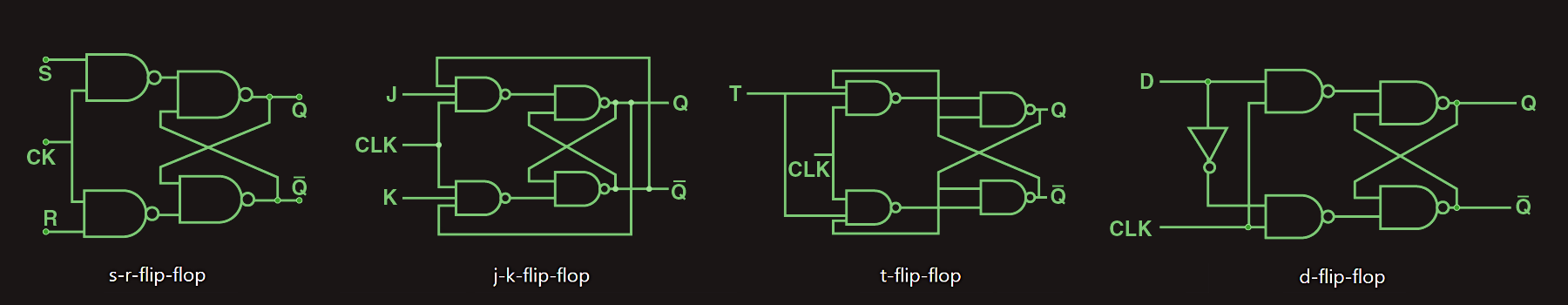
The illustration below, for example, shows the circuit for an SR latch designed with NOR gates. An SR latch can also be constructed with NAND gates, and those designs always have the S input on top and the R input below. An SR latch with NOR gates always has the R input on top and the S input below. In both designs, the output Q is always on top and the output Q-Inverted is always below. 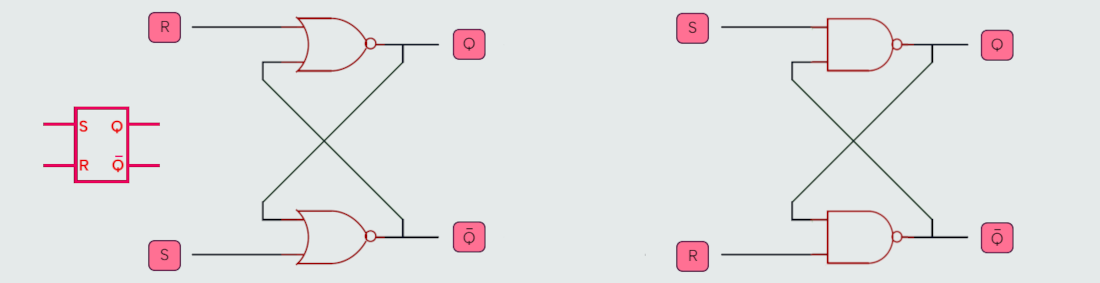
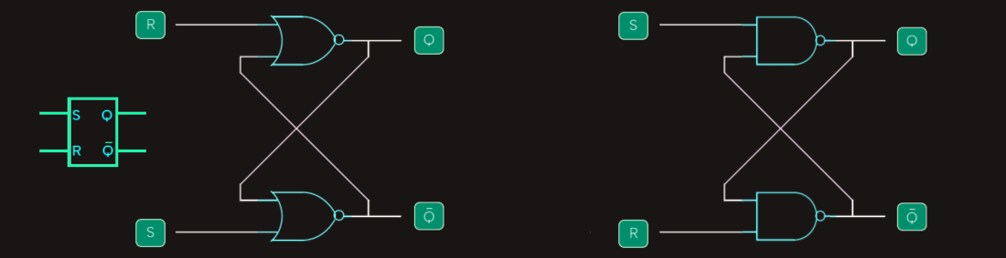 The SR latch consists of two NOR gates cross-coupled so that the output of each NOR gate is one of the inputs of the other NOR gate. There are two inputs, an S input to set the latch, and an R input to reset the latch. On the output side, the latch is considered to be ‘set’ when Q is high (then Q-Inverted is automatically low), and ‘reset’ when Q is low (then Q-Inverted is automatically high). In order to trigger a latch to change its state, short pulses of signals are sufficient at the input lines.
Flip-Flops
In clocked sequential logic circuits, flip-flops are used to store one bit of data. With regard to the basic operating principle, a flip-flop is comparable to a latch. However, the fundamental difference between the two is that a flip-flop ensures that the output doesn’t change more than once during a single clock cycle. This is achieved by linking two latches in series so that the outputs of the first latch are used as the inputs of the second latch. A clock signal is used for both latches, whereas the clock signal for the second latch is inverted.
The two inputs S and R are used to set and reset the flip-flop respectively. The clock input is used to control both the master and slave latches. Therefore, the master latch is connected to the ‘original’ clock signal whereas the slave latch is connected to an inverted clock signal. The inversion of the clock signal is what actually prevents the flip-flop from becoming transparent.
Flip-Flop has two stable states: SET and RESET. The ‘set’ state is when the output of the circuit is 1, and the ‘reset’ state is when the output is 0. A flip-flop can be triggered to change its state by applying a pulse or signal to its input. When the input signal is applied, the output of the flip-flop will change to the opposite state. For example, if the flip-flop is in the ‘set’ state, applying a signal to its input will change its state to ‘reset.’ Flip-Flops use two feedback loops — the ‘set’ loop and the ‘reset’ loop — which connect to the flip-flop’s inputs to store data. The input signals determine the specific output state of the flip-flop.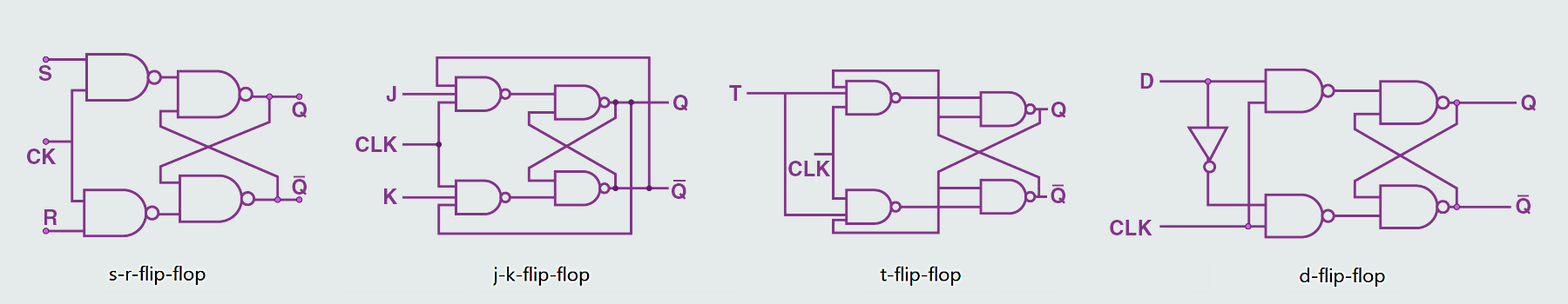
 Flip-Flops (basic building block of a flip-flop is a latch, which is a circuit that can store a single bit of data) are essential building blocks in digital electronics. From synchronizing signals between different parts of a circuit to creating counters, shift registers, and memory units, they allow us to store and manipulate binary data, which is the foundation of all digital systems.
Registers
We know that a flip-flop is a tiny device that can be used to store 1 bit of data. If the device needs a higher storage capacity in terms of the numbers of bits, the number of flip-flops needs to be increased. The number of required flip-flops is identical with the number of bits the device intends to store. Such a device that contains a certain number of flip-flops is called a register.
The binary data stored in a register can be moved from one flip-flop to another. Devices that allow such types of data transfers are called shift registers. A shift register is an array of flip-flops in which the output of each flip-flop is connected to the input of an adjacent flip-flop. All flip-flops share the same clock, so one clock cycle can shift all data by one position at the same time. Shift registers can have both serial and parallel inputs and outputs. 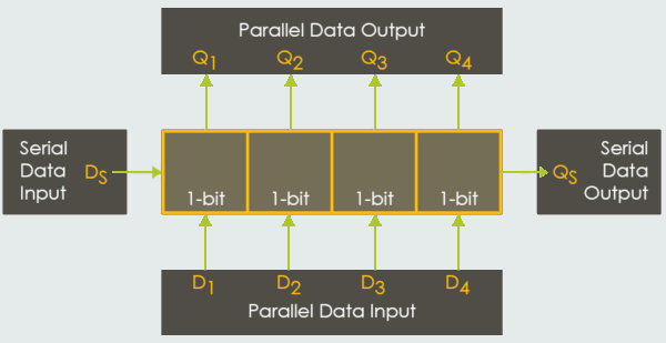
 Depending on the circuit design, serial data can be shifted in two directions, left or right. This means that the left serial input can also be an output, and the right serial output can be an input. The various input and output options lead to the following categories of shift registers:
· Serial Input Serial Output (SISO)
· Serial Input Parallel Output (SIPO)
· Parallel Input Parallel Output (PIPO)
· Parallel Input Serial Output (PISO)
· Universal Shift Register
A universal shift register can store data from serial or parallel inputs, shift data in both directions, and output data through serial or parallel outputs. Universal shift registers are very useful circuits, and therefore they are also produced as individual microchips.
The Bus System
The bus is an internal communication system within an integrated circuit. It is a set of parallel electrical wires that transports information between individual registers. Numerous registers and other components typically share the same bus, and therefore it is also referred to as ‘common bus’. For each bit position within the registers the bus contains a separate wire. For instance, one wire of the bus system is exclusively used to carry information from the bit position “0” of all registers, another wire is only used by the bit position “1” etc. Naturally, it doesn’t work to carry the information of all registers at the same time. Therefore, to coordinate the communication between the registers and the bus system, additional control structures are required. 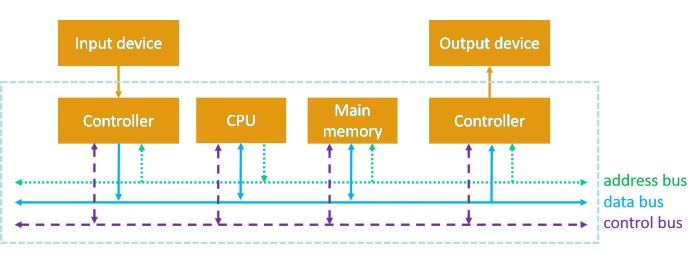 For information to be transferred from a source register to the bus, the register’s outputs have to be connected to the individual bus wires. However, if information from more than one register must be transmitted to the bus, the outputs of the source registers cannot simply be connected to the same line. This is due to the fact that the output lines of registers always have their stored values present, and connecting more than one register output to the same wire will result in a short circuit if both output signals are different from each other.
As a solution to this problem, additional hardware and control signals are used to determine which source register is selected by the bus system at a particular time.
One solution to design a common bus system is to use multiplexers. Alternatively, a common bus system can also be designed with tri-state buffers.
In case that registers need to read information from the bus, their inputs can be directly connected to the bus without hardware inbetween. This is due to the fact that registers can independently turn reading off or on, which is different from their writing function where stored bits are always available at the output.
The Microarchitecture Level
The microarchitecture level is a further abstraction where the overall interaction of all functional units is described. The abstraction lies in the simplification of schematics where only simple block diagrams and arrows are used, but auxiliary circuitry like multiplexers or tri-state buffers are usually not shown. In general, microarchitectures are typically categorized into two parts: The datapath which performs the calculations and microoperations (register transfer, arithmetic, logic, shifting) on data, and the control unit or control path which sends sequences of control signals to the datapath for processing. 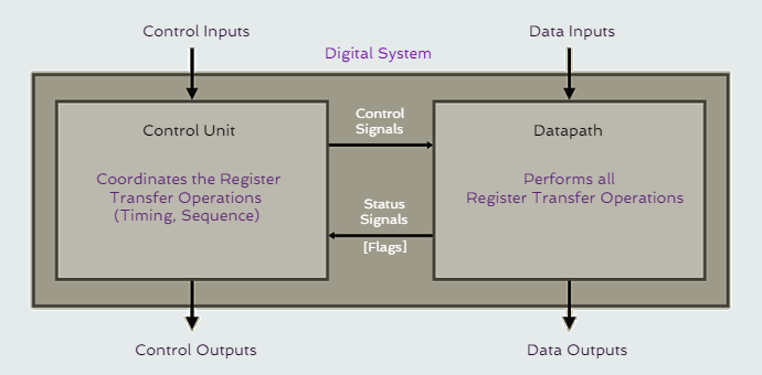
 The datapath contains three types of units which can be categorized into storage units (registers), functional units (ALU, adders) that perform all the necessary operations on data, and interconnect units (buses) including their corresponding driver circuits (multiplexers, tri-state buffers). The datapath can also be described as the path that the input data follows in a CPU until it appears as an output.
The control unit includes circuits that issue instructions to the datapath to coordinate data transfers, operation selection, and other actions.
The System Level
The system level is an abstraction where the CPU is not viewed from the inside with all the control systems and functional units, but it is simplified and visualized as a complete and finite device with certain functionalities and characteristics. What is relevant on this level of abstraction is the device's input / output requirements including power supply and clock, its operating behavior including instructions that the device can understand and execute, performance limitations, its temperature range, package requirements, and others.