


The Device Level - Transistor Level
A transistor is a device that uses smaller input signals to regulate larger current flows.
Transistors have these general modes of operation:
1. Cut-off Region: When a transistor is working in the cut-off region, the current flowing through the transistor is zero. In this mode, the transistor is in the ‘OFF’ state and acts like an open circuit.
2. Active Region: The transistor is ‘ON’ but hasn’t reached its highest current yet. This means, variations in the small input current will become noticeable in a higher variation of the output current. While in this mode, the transistor acts as an amplifier.
3. Saturation Region: The transistor is in the ‘ON’ state and acts like a closed switch.
It depends on the transistor type what is required to switch it on or off, but it is typically a minimum current established between two pins of the transistor or a voltage applied between two pins.
The ability to amplify analog signals is a required effect in many audio and radio applications. In digital circuits, however, signals consist of ‘1’ and ‘0’ which are realized by the presence of either full supply voltage (for instance 12V = ‘1’) or ground voltage (0V = ‘0’). Therefore, transistors as used in digital integrated circuits do only act in the cut-off region (completely off) or saturation region (completely on). For that reason, transistors in digital integrated circuits can be imagined as simple switches that either open a circuit (switch is off) or close it (switch is on).
In the early stages of transistors, germanium was a popular semiconductor material that was used in transistor production. During the 1960s and 1970s, germanium was gradually replaced by silicon due to several reasons; there are some advantages of silicon that made production and handling of transistors easier. In rare cases for special applications, gallium arsenide is used as a compound semiconductor material as it has some better properties for high frequency applications.
So, the starting material for almost all transistors is silicon, a semiconductor material which has very special electric characteristics. In its pure form, silicon does not conduct electricity very well. However, by a process called doping, impurities are injected into the material, effectively adding or removing electrons from the silicon. If electrons (which are always negative) are added, this type of silicon is referred to as n-type (negative type) silicon. If electrons are removed, this type of silicon is called p-type (positive-type) silicon.
If a layer of n-type silicon is next to a layer of p-type silicon, these two different zones form a connection that is called the p-n junction. The special property of the p-n-junction is that it is conductive in one direction (if a minimum voltage is applied in one way) but blocks the flow of electricity in the opposite direction (if a minimum voltage is applied in another way). Conductivity of a p-n-junction can also be increased if an electric field is applied.
Some transistors are designed primarily for amplification purposes, some are designed for switching purposes and some transistors are designed for both amplification and switching purposes. Depending on their structure, transistors can be categorized into one of the two main types: Bipolar Junction Transistor (BJT) and Field Effect Transistor (FET) - Enhancement Mode Metal Oxide Field Effect Transistors (MOSFET).
Bipolar Junction Transistors – BJT
Bipolar junction transistors are current-controlled devices. If a small amount of current flows through the base, a BJT transistor allows a larger current flow between the emitter and the collector. It depends on the type of BJT in which direction current needs to flow through the base in order to turn the transistor on.
All bipolar junction transistors are formed by three alternating layers of silicon, either a layer of p-type silicon inbetween two layers of n-type silicon (NPN type) or a layer of n-type silicon inbetween two layers of p-type silicon (PNP type). They use both positive and negative charge carriers, hence the name bipolar. All bipolar junction transistors have three terminals, called emitter, base and collector.
An NPN transistor is the one in which two layers of N-type semiconductor material are separated by a thin layer of P-type semiconductor material. Hence, in case of NPN transistor, the emitter and collector are of N-type while the base is of P-type. When a thin layer of N-type semiconductor material is sandwiched between two layers of P-type semiconductor material, the resulting transistor is known as a PNP transistor. In a PNP transistor, the emitter and collector are made of P-type semiconductor material while the base is made of N-type material.
NPN transistor is more preferred as compared to PNP because in PNP holes are the majority charge carriers whereas, in NPN electrons are the majority charge carriers. Switching of NPN transistor is faster due to high drift velocity of electrons. Switching speed of PNP transistor is low due to low drift velocity of holes.
One of the main differences between these two transistors is that in the NPN transistor, the flow of current will be in between the collector to emitter terminal once the positive supply is provided to the base terminal of the transistor. In the PNP transistor, the charge carrier supplies from the emitter terminal to the collector once a negative supply is provided to the base terminal.
There are various differences between NPN and PNP transistors. Both of these transistors are widely used in different electronic applications like in switching and amplification, etc. Thus, the knowledge of these differences can help an individual to select the right kind of transistor as per the exact requirements.
For integrated circuits, transistors are being produced in a planar design so that they have all their electrically active areas (connector terminals) on the surface of the silicon substrate. The layout of the planar NPN transistor is called vertical. None of the PNP transistors can match the performance of the vertical NPN transistor. In addition, NPN transistors are cheaper in production and smaller in scale. Another reason is that it is more convenient for circuit designers to have the emitter tied to ground so that the control signal is always relative to ground. For these reasons, NPN type transistors are more popular than PNP types.
Field Effect Transistors – FET
Field Effect transistors are voltage-controlled devices. They only require voltage applied to the controlling terminal to turn the FET either on or off. The voltage (instead of a current) applied induces an electric field to control the flow of current through the device.
The terminals of field effect transistors are called source, drain and gate, which roughly correspond to the emitter, collector and base terminals of bipolar junction transistors. The gate terminal may be thought of as controlling the opening and closing of a physical gate. Field effect transistors are also known as unipolar transistors since they involve single-carrier-type operation. That is, FETs use positive or negative charge carriers in their operation, but not both.
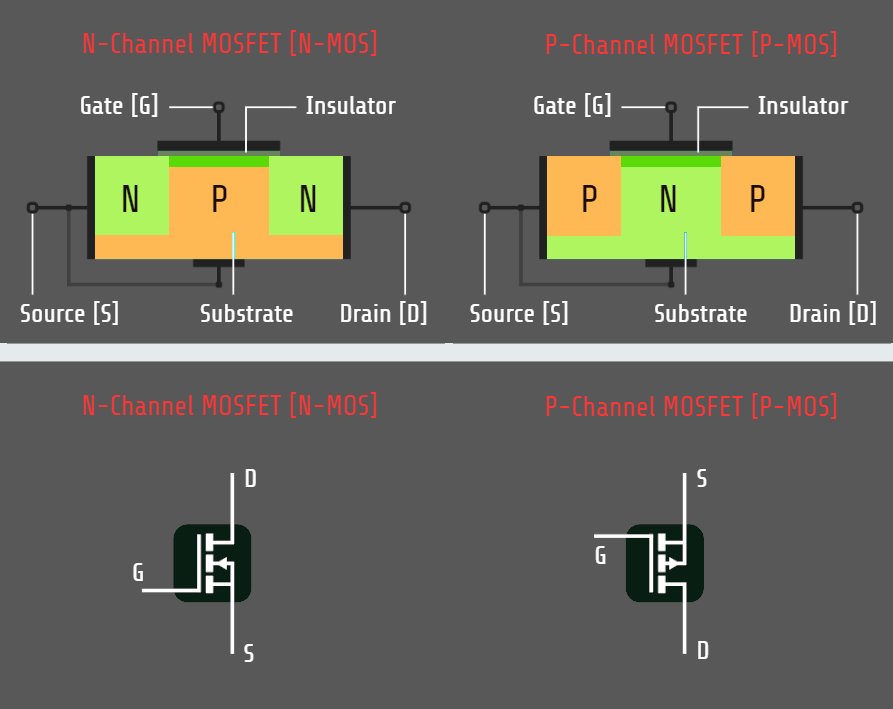
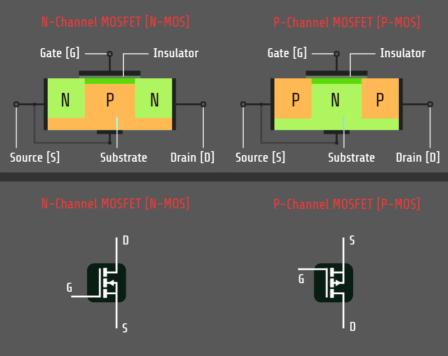
Both MOSFET's function is the same, but they differ primarily in their internal structure. In a P-channel MOSFET, the internal structure is made so that the conductive channel is made of P type, while in an N-channel MOSFET, the conductive channel is made of N type. For a P-channel MOSFET, a negative voltage must be applied to the control electrode for proper operation. With an N-channel MOSFET, it is necessary to apply a positive voltage to the control electrode in order to work properly.
The MOSFET is mainly used as an electronic switch or amplifier where a certain voltage is used to pass and control the flow of current of a different voltage. Various integrated circuits such as microprocessors and memory devices contain thousands to a million integrated MOSFET transistors on each device, providing the basic switching functions necessary to implement logic operations and data storage. Various electronic circuits containing MOSFET transistors are widely used in applications such as power supplies, variable frequency drives, and other power supply applications where each device can control power of up to 1000W. Radio frequency amplifiers that operate up to very high frequencies (UHF spectrum) use MOSFET transistors as power amplifiers. Radio systems also use MOSFET transistors as oscillators.
MOSFETs to be used in integrated circuits, must also have all their connector terminals on one side of the surface, and therefore they are typically designed in a planar shape.
One of the most significant advantages of field effect transistors is the low power consumption which makes them a favorite in today’s integrated circuits with millions and billions of transistors. FET only requires power when actively switching, but there is almost no power consumption when not used for switching. Some other advantages of field effect transistors is that they can be produced at a higher packing density, which means that the dimensions of FET devices can be scaled down more easily compared to BJTs, also reducing production cost of FETs. In addition, field effect transistors offer a greater thermal stability and lower noise levels than junction transistors. Conversely, field effect transistors are more susceptible to damage by electrostatic charges while handling.
The Circuit Level
An electrical circuit is a network of electrical components such as power sources, resistors, switches, transistors, light emitting diodes, and others. When the circuit is closed, this network always consists of a closed loop, allowing charge carriers to flow through the components (called the ‘load’ of the circuit) and return to their power source.
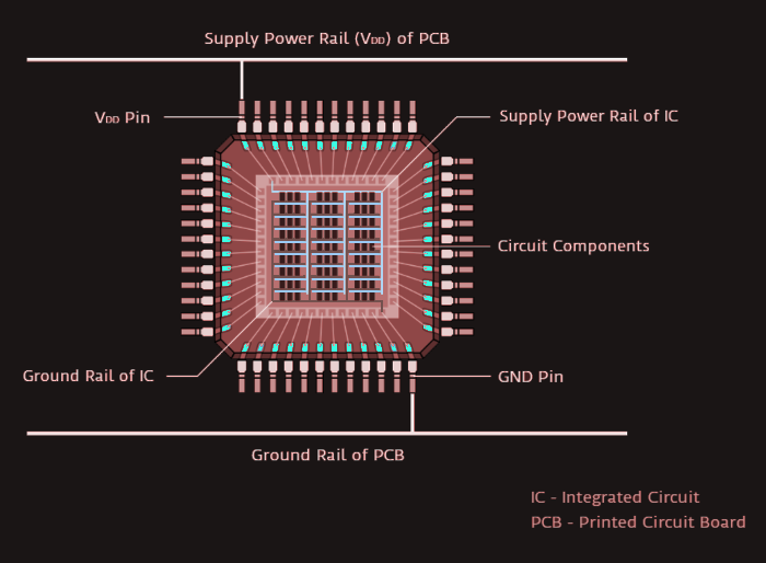
In integrated circuits, the power supply is always provided from external sources, for instance a computer’s power supply unit. The main power supply unit provides power to all components of the appliance through a network of power lines, conductive tracks called ‘power rails’, that are on or inside the appliance’s printed circuit board. For its own voltage supply, every microchip has at least two power supply pins that direct the external supply voltage into the chip.
One is always the positive supply voltage pin, labeled VCC or VDD. This one is connected to the positive power supply rail of the appliance’s printed circuit board. Inside the chip, the positive power supply is distributed to the required areas through internal power rails. There are industry standard voltage levels for integrated circuits with supply voltages from 0.6V up to 12V. Another pin is always the ground pin, labeled GND. This one is connected to the ground rail of the appliance’s printed circuit board. The ground rail usually is the most negative voltage level (typically 0V), and is the return path of an electrical circuit. The ground rail inside the microchip leads away from all the tiny circuits to the ground pin of the microchip, into the ground rail of the appliance’s printed circuit board, effectively closing the circuit. Circuit designers often use VEE or VSS instead of GND to indicate that the respective rail has the most negative voltage of the entire integrated circuit. There can be some exceptions, but in most cases, the lowest voltage in an integrated circuit is 0V, and therefore equivalent to GND.
The letters D and S refer to drain and source, and the letters C and E refer to collector and emitter, depending upon the type of components in a circuit.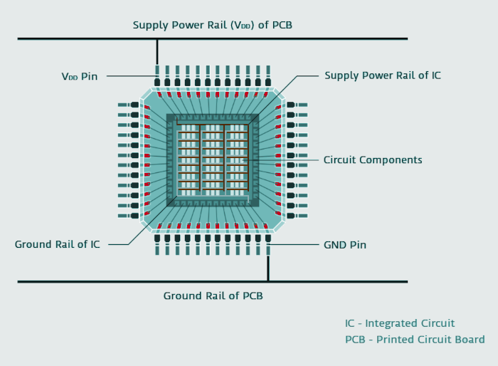
 So, the circuit level is a level of abstraction that makes it irrelevant to think about the physical structure of individual transistors with all their different materials and specialties. Instead, transistors are only thought of as small switches and a circuit designer only needs to know their general working principles.