


A diode is so called because it has two terminals: the anode, the positive terminal, and the cathode, the negative terminal. In the case of a p-n junction diode the anode is the p-type and the cathode is the n-type. We have learned earlier that diode will conduct in one direction but not in the other. A diode is an electrical equivalent of a check valve. In plumbing, a check valve allows water to flow in one direction only. Any water trying to flow in the opposite direction is stopped by a closed valve. A diode works the same way with current.
So, a diode is made of two types of semiconductors pushed together. They are known as type P and type N. They are created by a process called doping. In doping the silicon, an impurity is created in the crystal that affects the structure of the crystal. Some dopants will create a type N structure in which there are some extra electrons simply hanging out with nowhere to go. Other dopants will create a type P structure in which there are missing electrons, also called holes. So we have one type N that will conduct negative charges with a little effort. We have another type that not only does not conduct but actually has holes that need filling. 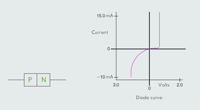
 Due to the interaction of the holes and the free electrons, a diode allows current to flow in only one direction. A perfect diode would conduct electricity in one direction without any effect on the signal. In real world, a diode has two important characteristics to consider:
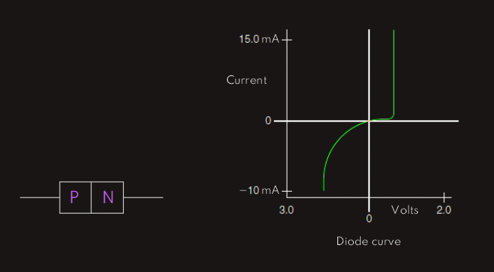
1. the forward voltage drop and
2. the reverse breakdown voltage
The forward voltage is the amount of voltage needed to get current to flow across a diode. This is important to know because if we are trying to get a signal through a diode that is less than the forward voltage, we will be disappointed. Another fact is that the forward voltage times the current through the diode is the amount of power being dissipated at the diode junction. If this power exceeds the wattage rating of the diode, we will soon see the smoke come out and the diode will be burnt.
Although a perfect diode could block any amount of voltage, the fact is, actually, that every diode has its price. If the voltage in the reverse direction gets high enough, current will flow. The point at which this happens is called the breakdown voltage or the peak inverse voltage. This voltage usually is pretty high, but it can be reached, especially if we are switching an inductor or motor in our circuit.
There is a type of diode called a zener in which this breakdown voltage is controlled and counted on. A Zener diode is a special type of rectifying diode that can handle breakdown due to reverse breakdown voltage without failing completely. A Zener diode is a silicon semiconductor device that permits current to flow in either a forward or reverse direction. The diode consists of a special, heavily doped p-n junction, designed to conduct in the reverse direction when a certain specified voltage is reached. The Zener diode has a well-defined reverse-breakdown voltage, at which it starts conducting current, and continues operating continuously in the reverse-bias mode without getting damaged. Additionally, the voltage drop across the diode remains constant over a wide range of voltages, a feature that makes Zener diodes suitable for use in voltage regulation. The major application for these devices is to limit or stabilize a voltage between two points in a circuit.
The forward characteristic for a zener diode will be the same as for any other p-n junction diode, and also, since the device is always used in its reverse bias mode, only its reverse characteristic is shown on figure below. 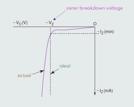
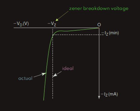 Vz represents the zener breakdown voltage, and if it were an ideal device, this p.d. across it would remain constant, regardless of the value of current, Iz, flowing through it. In practice the graph will have a fairly steep slope as shown. The value of current that may be allowed to flow through the device must be limited so as not to exceed the diode power rating. This power rating is always quoted by the manufacturer, and zener diodes are available with power ratings up to about 75 W.
Transistors
Transistors are three terminal semiconductor devices that are primarily used for two purposes:
1. switching and
2. amplification
One terminal of the transistor is typically used as a control terminal.
Switching
In their natural state, transistors tend to either act like open circuits or short circuits, depending on the type. So, they either easily allow or readily block current flowing through their two main terminals. By applying a voltage or current to the input terminal, it’s possible to reverse the transistor into the opposite mode it started in. In this fashion, the transistor acts like a switch. ![]()
![]() The transistor does not allow current to flow when no voltage is applied to its input. With 5V applied to the input, current can now flow through the transistor.
The transistor does not allow current to flow when no voltage is applied to its input. With 5V applied to the input, current can now flow through the transistor.
Amplification
Transistor amplification happens when a voltage or current is applied to the input that is in between the on and off states of the switching application. Following our previous example, we would find that the amount of current that flows through the transistor depends on the voltage applied to the input. For example, a 1V at the input may allow 20mA of current to flow, 2V may allow 40mA, 3V may allow 60mA. 5V and above may only allow 80mA of current to flow.
This region of the transistor, between its on and off states, is known as the active region.
Depending on the type of transistor, we can use this region to get a large output from a small input.
In our example, the 20mA output from the 1V input can be passed on to a 100 Ohm resistor, creating an output U=I·R. 1V at the input of the transistor is amplified to create 2V at the output.
If we have a couple of diodes tied together, we will get the next type of semiconductor, which is made by tacking on another type P or type N junction to the diode structure. It is called a BJT, short for bipolar junction transistor, or just transistor. Middle part is also known as the base of the transistor. When a current is applied to the base, the junction is energized and current flows through the transistor (like the diode, charges from the base connection fill up the depletion region and thus current can begin flowing). The other connections on the transistor are called the collector and the emitter. There are two types of these transistors: NPN and PNP transistors.
Another semiconductor transistor is the Field Effect Transistor, or FET. Much like the BJT, a FET has three terminals known as the Gate, Drain, and Source. The two most common types of FETs are the Metal Oxide Semiconductor FET (MOSFET) and the Junction FET (JFET).