


Many computer components are designed to use 5 Volts DC. Now, the question is how to get the voltage value we want out of our rectifier...
The easiest and most conventional way is to use a transformer on the AC source side to change our incoming AC waveform into a smaller voltage waveform so that the rectifier output gives us the desired voltage. For example, we may use a transformer that converts 120VAC into 12VAC before it goes into rectifier. By the time it gets out of the rectifier, the output may be close to what we are looking for (5VDC). Then we can use some resistors to trim this DC voltage slightly in order to achieve our final desired voltage. This is the way how rectification was done, historically, because there are some issues here:
• AC power that is delivered at 60 Hertz implies that AC transformers used to convert 60 Hertz power from one voltage to another are bulky and heavy.
• Using resistors within the rectifier causes some power loss, making the overall power supply less efficient.
• The capacitors used to keep the DC output relatively smooth are large and heavy, as well.
Modern day power supplies make use of a technique known as high frequency switching.
A high frequency switching power supply eliminates the bulky transformer that normally would take the 120VAC and change it to somewhere around 12VAC before it was rectified. Instead, the 120VAC is directly rectified to DC without the transformer. At this point, we have rectified high voltage DC. The next stage of the power supply feeds this DC voltage to high frequency switching transistors that cycle on and off very fast and this fast switching essentially turns the DC back into a very high frequency AC signal. The high frequency AC signal is then delivered to a transformer that converts the voltage down to a level that is desired at the output of the supply. This final AC voltage is rectified and filtered a second time to create a final DC output voltage.
What is done here is because higher frequency AC signals require smaller and lighter transformers, as well as smaller and lighter capacitors for the rectifiers. Special circuitry within the supply also can tightly control the output voltages to very precise levels.
Bus Voltages
The power supply converts the voltage coming from the wall socket into the voltages that are usable by the computer devices.
Most computer device manufacturers have standardized their equipment to utilize commonly available power within the computer. A typical computer power supply delivers multiple voltages, including +12, +5, +3.3, -5 and -12.
The supply creates these voltages on three separate lines, or busses, that the equipment can attach to ones of these lines and use the appropriate voltage. A device’s manufacturer will specify how and where to connect power to each device.
We see that while some supplies provide -12V and -5V power, there typically isn’t a supply of -3.3V power available. This is because the use of negative voltages from the power supply is slowly being phased out, since in many cases the relatively small number of devices that still use negative voltages can generate them internally without the general need for a common bus. When +3.3V became a standard supply voltage, it was decided to not provide a -3.3V counterpart that would eventually just be phased out anyway.
Power from the supply is delivered to the various computer components via cables and connectors. Each peripheral inside of the computer has some connection to get its power from the central power supply. Each component inside of the computer needs electrical power in order to function. The power consumption required by any individual component may be small, but when added up all of the components inside of the computer may need a significant amount of power. Power supply is rated by its output power, in Watts.
A 350 Watt power supply isn’t always producing 350 Watts. This is a peak value that it is capable of producing, also known as instantaneous power. Most of the time it will be creating less power than this value. Each component manufacturer will specify a power rating for its device. This is generally how much power the device uses during normal operating conditions. Some devices may need to draw more power occasionally. Most power supply manufacturers take this into consideration and add extra capacity into the power supply to account for short bursts of extra power. This is generally specified as a peak power output.
Semiconductors
At the beginning of our "electrical journey" we saw that atom consists of a central nucleus containing positively charged protons, and neutrons, electrically neutral, surrounded by negatively charged electrons orbiting in layers or shells. Electrons in the inner orbits or shells have the least energy and are tightly bound into their orbits due to the electrostatic force of attraction between them and the nucleus. Electrons in the outermost shell experience a much weaker binding force, and are known as valence electrons.
In conductors it is these valence electrons that can gain sufficient energy to break free from their parent atoms. They thus become ‘free’ electrons which are available to drift through the material under the influence of an emf and hence are mobile charge carriers which produce current flow.
The shells are identified by letters of the alphabet, beginning with the letter K for the innermost shell, L for the next and so on. Each shell represents a certain energy level, and each shell can contain only up to a certain maximum number of electrons. This maximum possible number of electrons contained in a given shell is governed by the relationship 2n2 , where n is the number of the shell. 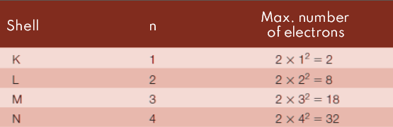 Semiconductors are group 4 elements, which means they have four valence electrons. The main features of a natural semiconductor are:
• A higher resistance than metal conductors, but a lower resistance than insulators.
• A valence number of +4.
The two most commonly used semiconductor elements are Silicon and Germanium. Their +4 valence numbers mean that they have a very stable covalent bond structure.
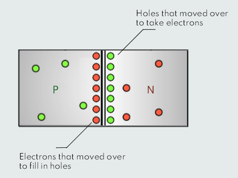
The usefulness of pure silicon as a semiconductor is limited. However, if we add small amounts of non-silicon material into the structure (this process of adding impurities to a semiconductor is known as doping) we will get extrinsic semiconductors, meaning they are not in their natural form, intrinsic semiconductors. Since a normal semiconductor has a valence of +4, a small amount of impurity will cause a charge imbalance. Doping a pure semiconductor with a small amount of material with a valence number of +5 creates an n-type semiconductor. It is referred to this because of the excess of free electrons in the material. Similiarly, we create a p-type semiconductor by doping a pure semiconductor with a small amount of material with valence number of +3. This results because of a hole that is left by the absence of an electron in the covalent bond structure.
Although the covalent bond is strong, it is not perfect. Thus, when a sample of silicon is at normal ambient temperature, a few valence electrons will gain sufficient energy to break free from the bond and so become free electrons available as mobile charge carriers. Whenever such an electron breaks free and drifts away from its parent atom it leaves behind a space in the covalent bond, and this space is referred to as a hole. Thus, whenever a bond is broken an electron-hole pair is generated. The atom which now has a hole in its valence band is effectively a positive ion because it has lost an electron which would normally occupy that space.
Doping a semiconductor does not add or remove any charge. The resulting product is still electrically neutral. Doping simply redistributes valence electrons so more or less free charges are available for conduction. At some stage the hole will once more be filled by an electron. This process is known as recombination, and when it occurs the normal charge balance of that atom is restored. The hole-pair generation and recombination processes occur continuously, and since heat is a form of energy, will increase as the temperature increases. This results in more mobile charge carriers being available, and accounts for the fact that semiconductors have a negative temperature coefficient of resistance, i.e. as they get hotter they conduct more easily. It must be remembered that although these thermally generated mobile charge carriers are being produced, the sample of material as a whole still remains electrically neutral. 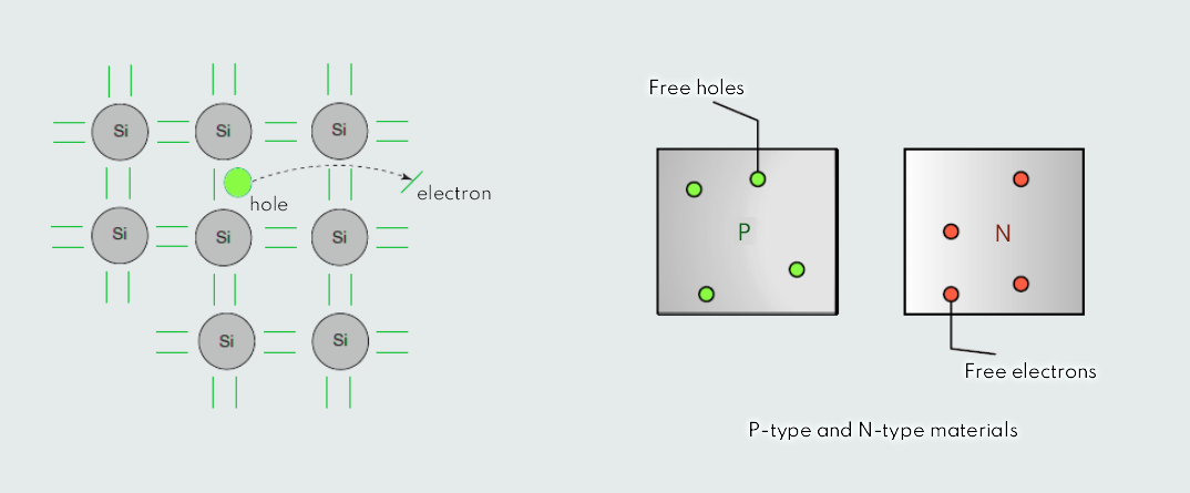
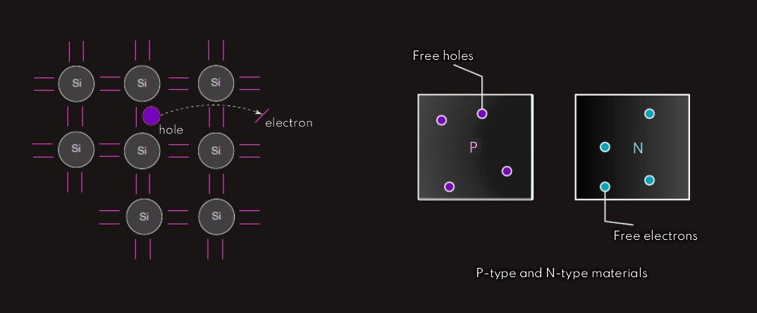 A hole really is a place where an electron could be, or moreso wants to be. If there is an electron nearby, it will jump into a hole and fill it up. Within the n-type semiconductor we think of electrons being the major current carrier. In the p-type semiconductor, holes are the major current carrier. The holes themselves cannot move — they are merely generated and filled. However, when a bond breaks down the electron that drifts away will at some point fill a hole elsewhere in the lattice. Thus the hole that has been filled is replaced elsewhere by the newly generated hole, and will appear to have drifted to a new location. In order to simplify the description of conduction in a semiconductor, the holes are considered to be mobile positive charge carriers whilst the free electrons are of course mobile negative charge carriers.
The PN Junction
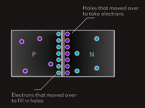
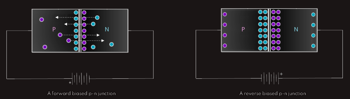
When we put a small piece of n-type semiconductor next to a small piece of p-type semiconductor, the extra electrons in the n-type conductor attempt to move over into available holes in the p-type conductor. At the same time, some of the holes in the p-type conductor end up moving over to the n-type to meet up with electrons. When this happens, we end up with an excess of electrons on the p-type side and extra electrons on the n-type side, creating an electrical imbalance. This electrical imbalance is known as the barrier potential and is shown above on the first figure. In silicon, this barrier potential is about 0.7 Volts.
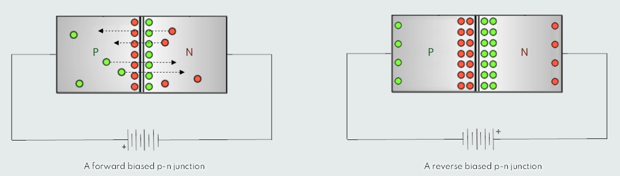
Now, when we apply an external voltage to p-n junction, depending on which direction we apply the voltage, we get what we call the forward and reverse bias, shown above, also.
If we apply a positive voltage to the p-type material and a negative voltage to the n-type material, we are applying a forward bias to the semiconductor. First, the negative voltage at the n-type material is going to attempt to push electrons towards the junction in the middle. The positive voltage at the p-type material will push the holes towards the barrier as well. This reduces the barrier potential. If the barrier potential is reduced enough, the charge carriers can move through the barrier and out the other side, which means that current flows.
Applying a reverse voltage to our semiconductor material is known as reverse bias. In this condition, the electrons are pulled away from the barrier on the n-type side and the holes are pulled away from the barrier on the p-type side, which results in a larger barrier and creates a much greater resistance for charges to flow through. The result is that no current flows through the barrier.